English
 English


Semiconductor manufacturing is an ultra-precision process with extreme requirements for cleanliness, thermal stability, electrical insulation, chemical resistance and plasma resistance. From wafer processing, lithography, etching and thin-film deposition to inspection and packaging, critical components inside production equipment are continuously exposed to corrosive specialty gases, plasma, strong acids and alkalis. These components must maintain dimensional stability at micron and even nanometer levels. Advanced ceramics such as high-purity alumina, aluminum nitride, silicon carbide and silicon nitride feature ultra-low outgassing, low thermal expansion, high thermal conductivity, plasma erosion resistance and reliable electrical insulation. They have become irreplaceable foundational materials for semiconductor equipment, supporting the continuous advancement of chip manufacturing toward smaller process nodes.
1. Wafer Handling and Chucking Components
Electrostatic chucks (ESC), wafer stages, ceramic suction plates, transfer arms and positioning pins are core parts for wafer processing, mostly fabricated from high-purity alumina or aluminum nitride ceramics. Aluminum nitride delivers outstanding thermal conductivity to realize fast and uniform temperature control over wafers, meeting strict temperature requirements for etching and deposition processes. Dense high-purity alumina minimizes particle shedding to maintain chamber cleanliness and reduce yield-killing defects on wafers. Ceramic locating pins and guides feature exceptional dimensional stability and resist deformation under repeated thermal cycling, ensuring accurate wafer alignment.
2. Chamber Components for Etching and Deposition
Chamber liners, focus rings, shield rings, gas nozzles and gas distribution plates used in etchers, PVD and CVD tools are subjected to intense bombardment and corrosion by fluorine-based and chlorine-based plasma. Ordinary metals are vulnerable to plasma attack and release metallic contaminants that ruin wafers. High-purity alumina and silicon carbide ceramics offer strong plasma resistance and superior chemical inertness with ultra-low metallic impurity levels. They reduce chamber contamination, extend component service life and cut unplanned downtime for equipment maintenance.
3. Thermally Conductive Insulating Substrates and Carriers
Aluminum nitride (AlN) ceramic is the preferred heat-dissipation substrate for power semiconductors, RF chips and IGBT modules. It combines excellent electrical insulation with high thermal conductivity. It isolates high-voltage circuits while rapidly removing heat generated by operating chips and preventing thermal failure. Alumina ceramic substrates are widely adopted for low-power chips, packaging carriers and sensor bases. They provide stable insulation at a competitive cost for discrete components and optoelectronic packaging.
4. Precision Motion and Vacuum Parts
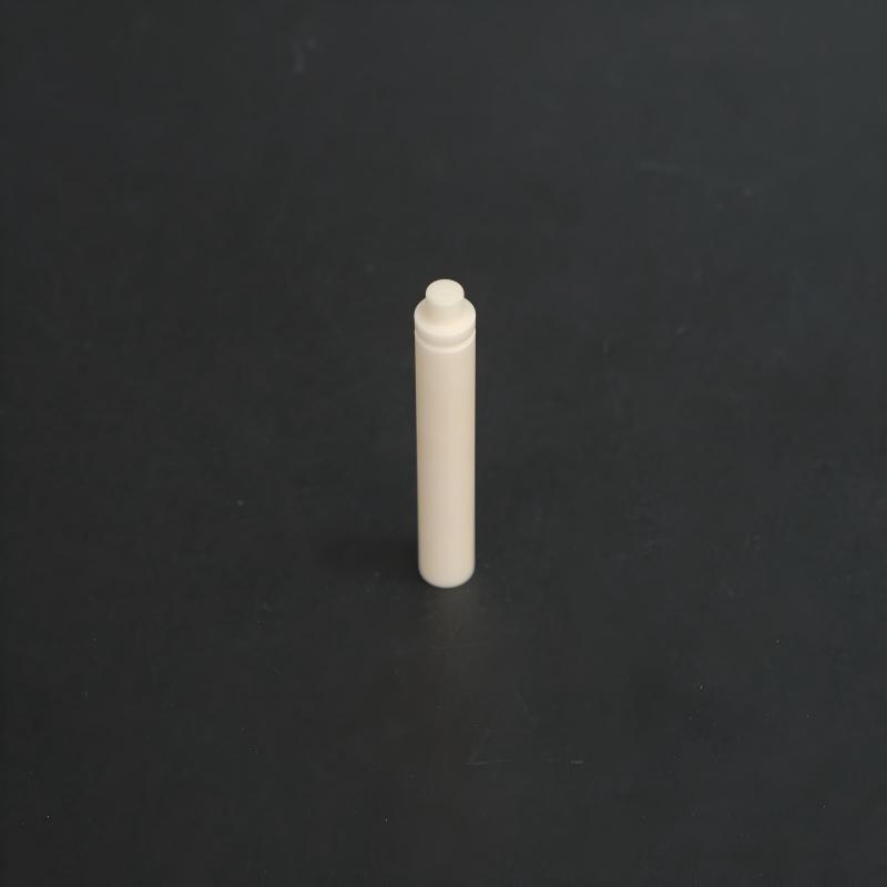
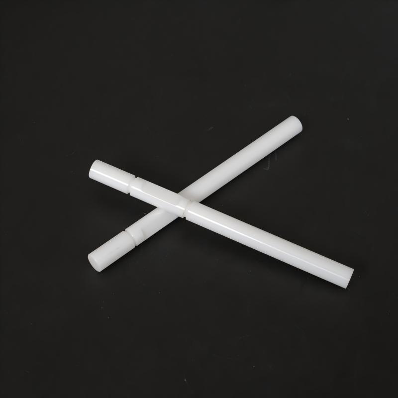
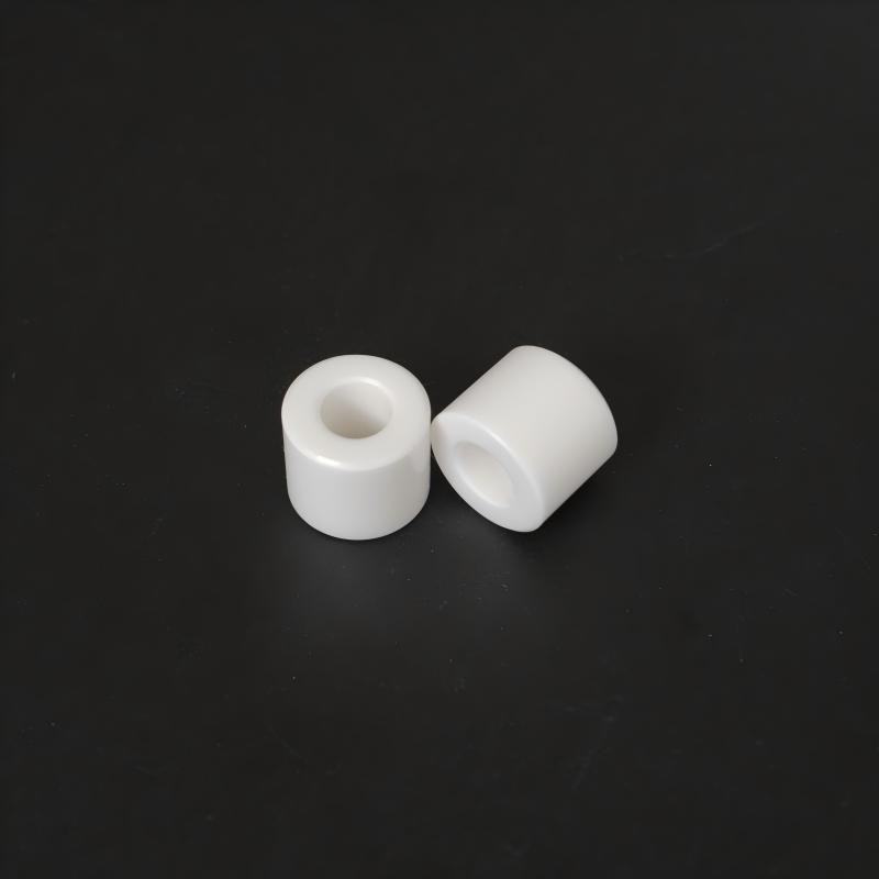
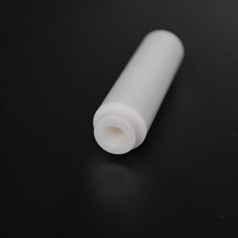
Advanced ceramics are widely used for vacuum flanges, insulating sleeves, ceramic shafts, bearings and thermal spacers inside semiconductor tools. Ceramic materials have extremely low outgassing rates, making them suitable for high-vacuum environments. Their thermal expansion coefficient is far lower than that of metals, so deformation under temperature fluctuation is negligible, securing repeat positioning accuracy for high-speed precision motion systems. Besides, non-magnetic ceramics fit inspection and metrology systems that demand magnetic-free working conditions.
5. Auxiliary Parts for Metrology, Lithography and Packaging
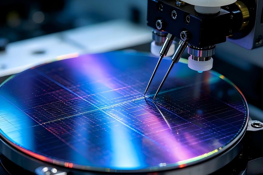
In optical inspection, lithography and probe testing processes, ceramics are made into probe cards, test carriers, optical reference blocks and thermal supports. Low thermal deformation avoids measurement drift caused by temperature changes. For packaging, ceramic packages and bases create hermetic, stable enclosures for MEMS devices and optical communication chips, protecting delicate chips from moisture, dust and external mechanical stress.
6. Industry Benefits and Outlook
The adoption of advanced ceramics helps reduce particle contamination on wafers and raise production yield, while improving equipment stability and lowering spare-part consumption. With the rapid development of advanced nodes such as 3 nm and 2 nm, as well as third-generation semiconductors including SiC and GaN power chips, market demand for ultra-high-purity, defect-free ceramic components keeps rising. The main challenges lie in ultra-high-purity powder preparation, ultra-precision lapping and forming of complex-shaped ceramic parts. In the future, toughened ceramic composites and near-net-shape forming technologies will further expand the application scope of advanced ceramics for semiconductor equipment.
Conclusion
Semiconductor manufacturing equipment across the whole workflow heavily relies on high-performance advanced ceramics. From wafer temperature control and plasma chamber protection, power heat dissipation substrates, to vacuum transmission, testing and packaging components, advanced ceramics integrate cleanliness, corrosion resistance, stable thermal performance, insulation and heat conduction. They serve as essential building blocks for state-of-the-art chip fabrication equipment.